How Solar Energy is Created
- Electrical current is a flow of electrical charge created by the movement of sub-atomic particles called electrons.
- A material like copper conducts electricity because it contains electrons that aren’t bound to any particular molecule and, hence, are capable of moving through it.
- Sunlight is composed of subatomic particles called photons. If a photon in a beam of light striking a conducting material has enough energy, it can “knock” any freely moving electron it impacts completely off the surface. This scientific process is called the Photoelectric Effect.
- We’re able to convert sunlight into clean, cost-free, and completely renewable energy to power your home because scientists and engineers, building on Einstein’s theory of light, created solar panels that channel the random Photoelectric Effect into a controlled scientific process known as the Photovoltaic Effect. That’s when the electrons impacted by sufficiently energized photons of light, instead of being randomly “knocked” around, get channeled into wires by an electrical force, creating DC electrical current.
Positive and Negative Charge
Besides electrons, which have a negative charge, the molecules composing matter also contain positively charged subatomic particles called protons. In its ideal state, a molecule’s total negative and positive charges balance each other out. But it’s possible for a molecule to acquire an extra electron, giving it a negative charge, or to lose one and wind up with a positively charged hole. Positively charged holes, are repelled by each other and attract negatively charged electrons. And, conversely, negatively charged electrons likewise repel each other and are attracted to positively charged holes.
Each solar panel is made up of several dozen wafer-like solar cells. Each cell is , in turn, composed of a negatively charged top layer containing additional electrons and a positively charged bottom layer containing holes where electrons are missing.
Two Types of Silicon
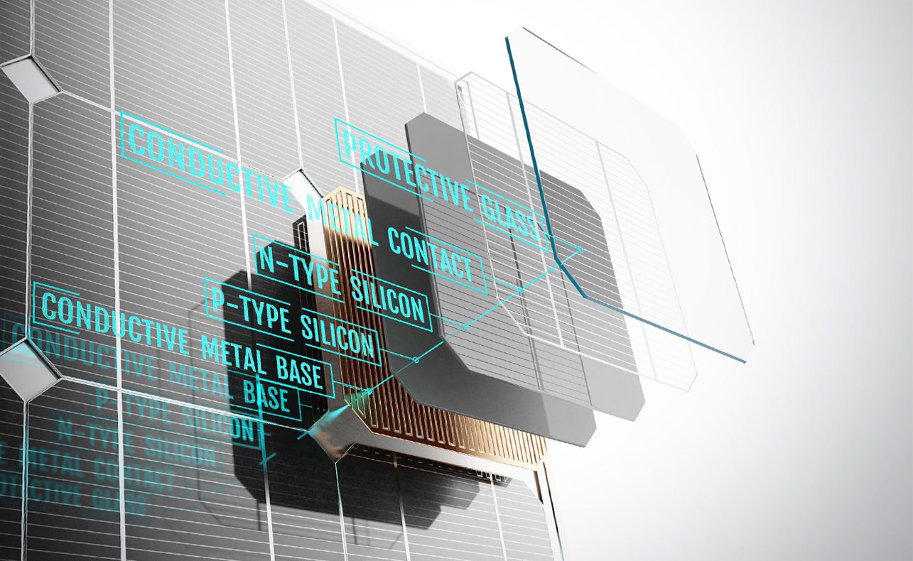
Two different types of silicon are generally used to make the two layers comprising a solar cell.
In its pure untreated state, silicon is like plastic. All electrons are tightly bound to their molecules, making it a very poor conductor. In a solar cell, however, the top layer is composed of N-TYPE silicon, which has been altered or doped by injecting phosphorus. Phosphorus has one more electron in its outer shell than silicon. So, phosphorus doping gives the top layer of a solar cell extra negatively charged electrons that are free to move around among its molecules.
The bottom layer of a solar cell, on the other hand, is made of P-TYPE silicon, usually doped with boron. Boron has one less electron in its outer shell than silicon. This creates positively charged holes in the bottom layer, which are also free to move around.
Though it’s easiest to think of the negatively charged n-type silicon being stacked on top of a separate layer of positively charged p-type silicon, in practice, any gap between the two layers will reduce the amount of electricity generated. So, to maximize efficiency, solar cells are constructed by taking a single slab of silicon and doping its top side with phosphorus and the bottom with boron.
The P-N Junction

The key to generating solar power lies in what happens in the region where the two types of silicon meet, called the p-n junction. Free electrons from the top layer of n-type silicon are attracted downward and start to fill holes in the bottom layer of p-type silicon. But, importantly, the process stops before all the extra electrons in the top cross to the bottom side.
Once the densely packed first layer of electrons transferred from top to bottom becomes large enough, their repelling force becomes so strong that it reaches across the newly created holes in the bottom layer of the n-type silicon above it and stops new electrons from entering.
Conversely, the newly formed holes in the top layer of n-type silicone repel any more holes from the bottom layer from moving up. At that point, a state of equilibrium is reached.
The top layer of electron-rich n-type silicon has developed a region at the bottom densely packed with holes; and the bottom layer of p-type silicon has a densely packed region at the top where all the holes have been filled by electrons. This combined boundary region forms the p-n junction.
Generating Current
Perhaps surprisingly, the top visible layer of a solar cell isn’t where the electrical current produced by sunlight is coming from. Instead, current is generated when some of the photons in sunlight pass completely through the top layer and strike the densely packed layer of electrons at the bottom of the p-n junction. Because electrical current is generated below the surface, the top layer of n-type silicon is heavily doped with extra electrons and very thin. That allows as many photons of light as possible to pass through. Whereas the bottom layer of p-type silicon is much thicker and more sparsely doped with holes. This makes the lower negatively charged layer of the p-n junction thicker, giving the photons passing through the thinner top layer of the cell plenty of opportunity to impact electrons. But even “much thicker” isn’t very thick when you’re talking about a solar cell; both layers together are still thinner than an eggshell.
Finally, a wire is run between the top layer of n-type silicon to the bottom layer of p-type silicone creating a circuit between them. If there were no circuit, when a photon of light impacted an electron in the lower part of the p-n junction, it would be attracted to the positively charged upper layer but eventually be repelled back to the hole it filled in the initial equilibrium state. However, the circuit running between the two layers allows the electron to be pulled through the p-n junction and back into the upper layer of n-type silicone. Equilibrium can be maintained by pushing another electron into the wire, which in turn eventually leads to an electron at the other end of wire re-entering the p-type bottom layer and rising back up to the p-n junction.
Thus, when a lot of photons from sunlight start continually impacting electrons in the lower half of the p-n junction, a flow of DC electrical current is created running through the wire connecting the top and bottom layers of the solar cell.
If you’d like to visualize the process in action, click the video link below.
https://www.youtube.com/watch?v=L_q6LRgKpTw
If you’d like to see the complex technology involved in combining dozens of solar cells into a single solar panel, click the video link below.
https://www.youtube.com/watch?time_continue=144&v=ckFieEHG7TU&feature=emb_logo